Graphene Synthesis By Cvd On Copper Substrates

Well Designed Substrates Capable Of Producing Large Single Crystal Bi Tri Layer Graphene Tech Explorist In 2020 Wellness Design Crystals Substrate
Https Ec Europa Eu Research Participants Documents Downloadpublic Documentids 080166e5c2e63475 Appid Ppgms

Regulating Top Surface Multilayer Single Crystal Graphene Growth By Gettering Carbon Diffusion At Backside Of The Copper Foil Abidi 2017 Advanced Functional Materials Wiley Online Library
C Free Full Text Recent Advancements On The Cvd Of Graphene On Copper From Ethanol Vapor Html

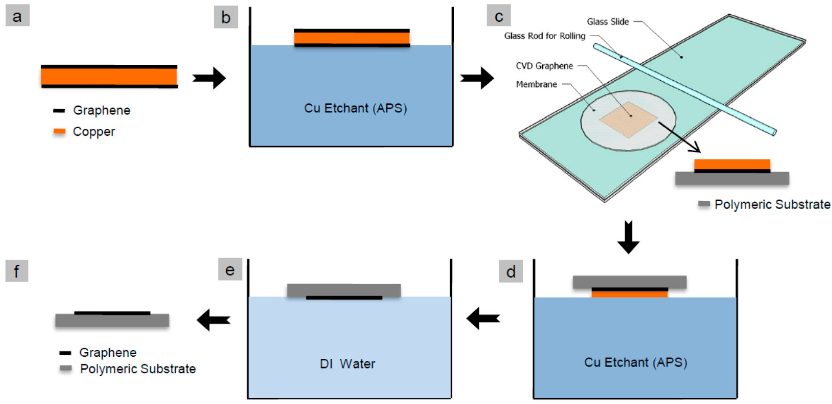
The Main Sources Of Graphene Damage At Transfer From Copper To Pet Eva Polymer Sciencedirect

Criteria For The Growth Of Large Area Adlayer Free Monolayer Graphene Films By Chemical Vapor Deposition Sciencedirect

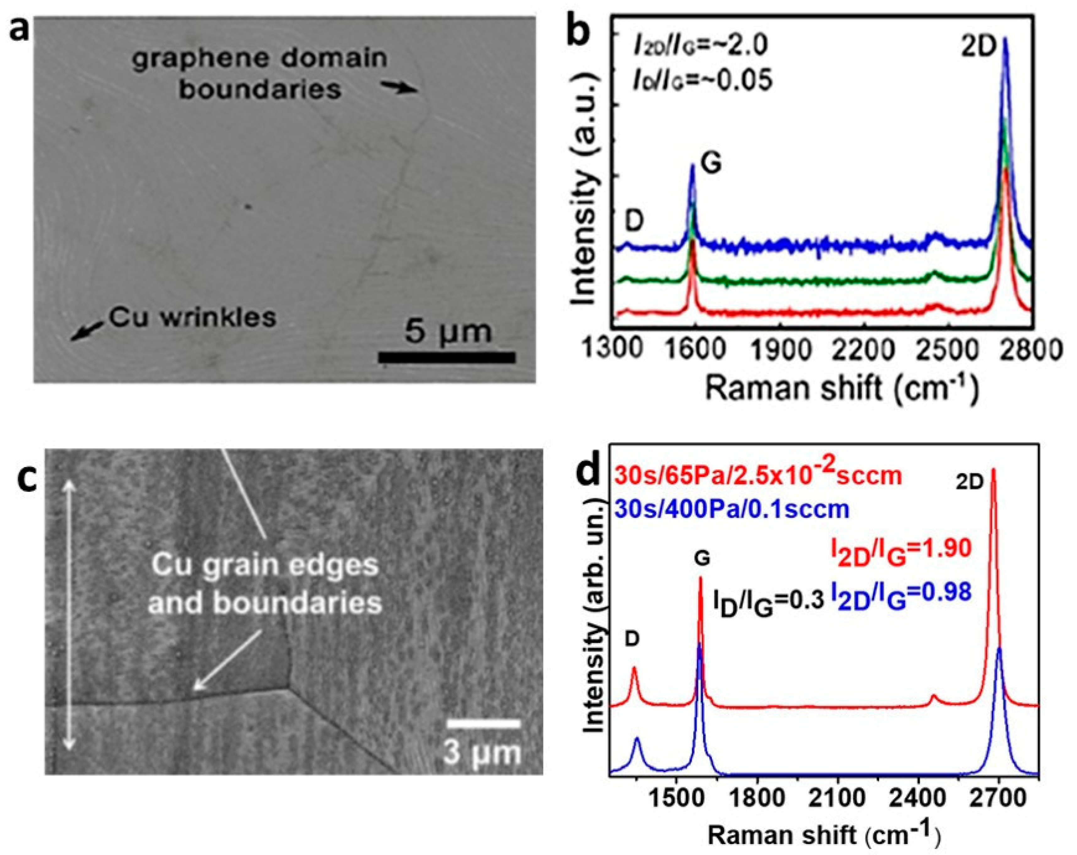
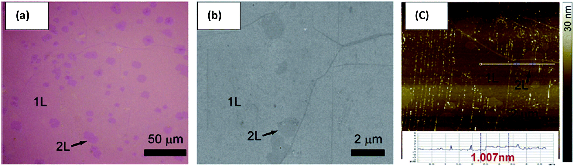
Various measurements showed predominantly uniform monolayer graphene.
Graphene synthesis by cvd on copper substrates.

Controlled Graphene Synthesis From Solid Carbon Sources Kondrashov 2019 Physica Status Solidi B Wiley Online Library

Vertical Graphene Nanosheet Vertically Grown Graphene Nanosheet Was Synthesized By Using Microwave Plasma Cvd Technique Here We Used The Gaseous Mixture Of A
Materials Free Full Text Synthesis Of Graphene Based Membranes Effect Of Substrate Surface Properties On Monolayer Graphene Transfer Html

Graphene Gas Sensor Fabrication A Schematic Drawing Of Graphene Download Scientific Diagram
Review Of The Synthesis Transfer Characterization And Growth Mechanisms Of Single And Multilayer Graphene Rsc Advances Rsc Publishing Doi 10 1039 C7ra00392g

Fundamental Limitations In Transferred Cvd Graphene Caused By Cu Catalyst Surface Morphology Sciencedirect
Pdf Graphene Cvd Growth On Copper And Nickel Role Of Hydrogen In Kinetics And Structure

Strain Relaxation In Different Shapes Of Single Crystal Graphene Grown By Chemical Vapor Deposition On Copper Sciencedirect

Direct Cvd Graphene Growth On Semiconductors And Dielectrics For Transfer Free Device Fabrication Wang 2016 Advanced Materials Wiley Online Library

Seamless Stitching Of Graphene Domains On Polished Copper 111 Foil Nguyen 2015 Advanced Materials Wiley Online Library

Low Temperature Growth Of Graphene Using Inductively Coupled Plasma Chemical Vapor Deposition Sciencedirect

Dancing Of Liquid Metal Droplets On Surface Of The Same Metal Pool Chinese Academy Of Sciences Metal Pool Liquid Metal

Graphene An Overview Sciencedirect Topics

Growth Of Single Crystal Graphene Arrays By Locally Controlling Nucleation On Polycrystalline Cu Using Chemical Vapor Deposition Wu 2011 Advanced Materials Wiley Online Library

High Yield Monolayer Graphene Grids For Near Atomic Resolution Cryo Electron Microscopy Biorxiv
Https Pubs Acs Org Doi Pdf 10 1021 Acsomega 8b03432

Optimisation Of Copper Catalyst By The Addition Of Chromium For The Chemical Vapour Deposition Growth Of Monolayer Graphene Sciencedirect

Direct Growth Of Graphene Film On Germanium Substrate Request Pdf
Https Iopscience Iop Org Article 10 1088 2053 1583 Aa5481 Pdf

Pdf Graphene Synthesis Properties And Application In Transparent Electronic Devices

Graphene Based Sensors Sciencedirect

Cvd Graphene On Sio2 Substrate Acs Material

Distributed Kalman Filtering For Time Varying Discrete Sequential Systems With Images Cyber Physical System Nanyang Technological University Control Engineering
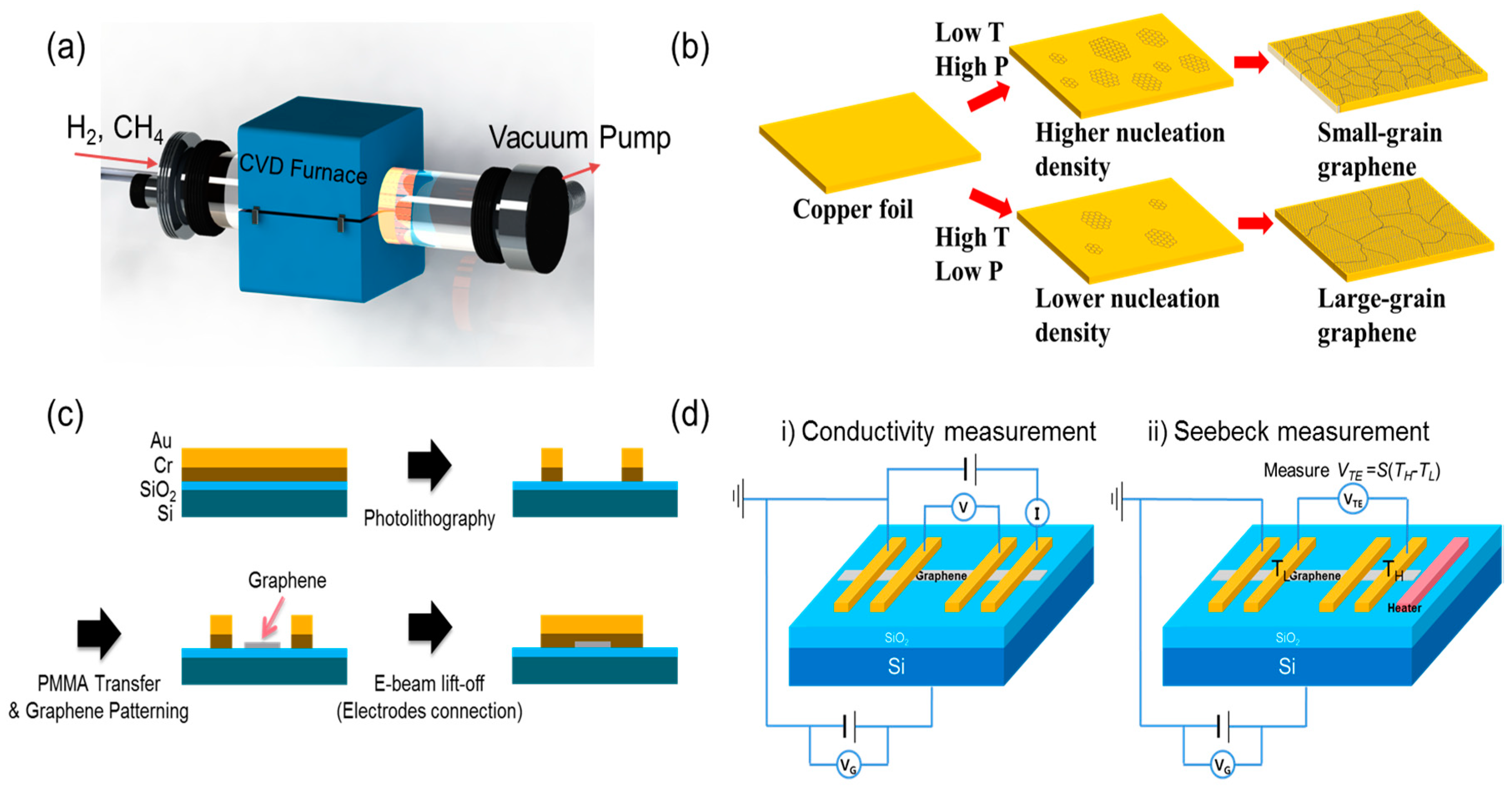
Nanomaterials Free Full Text Enhanced Thermoelectric Conversion Efficiency Of Cvd Graphene With Reduced Grain Sizes Html
Source : pinterest.com
